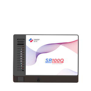
SR100Q Drive Circuit

| Performance indicators | Parameters | |
| Detectors* | Chip type and model* | Frontside-illuminated back-illuminated cooling HamamatsuS7031 |
| Effective pixels | 1024*122 | |
| Pixel size | 24*24μm | |
| Quantum efficiency | QE92%peak@650nm,83%@232nm | |
| Sensitive area | 24.576*2.928mm | |
| Electric parameter | Integral time | 1ms ~ 2100s |
| Data output interface* | USB3.0、RS232、RS485、20pin connector | |
| ADC bit depth* | 16bit | |
| Communication protocol* | Modbus | |
| Power supply | 5VDC 6A | |
| Operating current | < 4A | |
| Others | Operating temperature | 10°C ~ 40°C |
| Storage temperature | -20°C ~ 60°C | |
| Operating humidity | <90%RH (Non-condensation) | |
| Main control board size | 122mm*88mm | |
| Detector plate size | 70mm*40mm |
● High quantum efficiency: Chip 92%peak@650nm,83%@232nm
● High flexibility: Compatible with multiple interfaces including USB3.0、RS232、RS485
● Chip-integrated cooling: Long exposure faint signals clearly presents, strong environmental adaptability
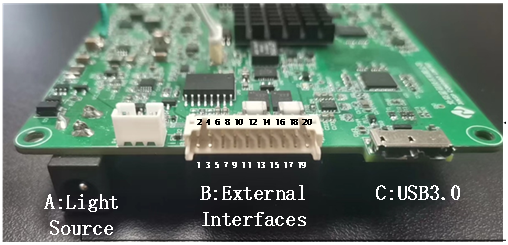
| Name | Type | Pin definition | |
| A | Power supply | DC 5V/6A | |
| B | External interface | 20PIN | As shown in the table on the right |
| C | USB3.0 | Default 485 electrical interface, can be configured as 232 by the host computer |
| PIN | Description | Type | Functional description |
| 1 | +5V | power | Input 5V power supply |
| 2 | +5V | power | Input 5V power supply |
| 3 | +5V | power | Input 5V power supply |
| 4 | +5V | power | Input 5V power supply |
| 5 | EGND | GND | Input 5V ground |
| 6 | EGND | GND | Input 5V ground |
| 7 | EGND | GND | Input 5V ground |
| 8 | EGND | GND | Input 5V ground |
| 9 | GPIO0 | IN/OUT | User-Defined input/output |
| 10 | GPIO1 | IN/OUT | User-Defined input/output |
| 11 | 485_GND | GND | RS-485/232 ground |
| 12 | 485_GND | GND | RS-485/232 ground |
| 13 | LB | IN/OUT | RS-485(N)/RS-232(RX-input) |
| 14 | LB | IN/OUT | RS-485(N)/RS-232(RX-input) |
| 15 | LA | IN/OUT | RS-485(P)/RS-232(TX-output) |
| 16 | LA | IN/OUT | RS-485(P)/RS-232(TX-output) |
| 17 | ISO_GND | GND | 9,10 19,20 pin ground |
| 18 | ISO_GND | GND | 9,10 19,20 pin ground |
| 19 | LAMP_EN | OUT | User-Defined output |
| 20 | EXT_TRIGGER_IN | IN | User-Defined input |
Write your message here and send it to us